No products in the basket.
Dereks Tech Tips – Issue 7

Top Tips for Micro, Electrical and Drag Soldering
In this month’s edition of Hakko Tech Tips, we will specifically look at micro soldering, soldering electrical components and drag soldering. We will also highlight how to combat electrostatic discharge, the importance of cleaning and look at different Hakko systems that can make light work of more challenging soldering operations.
- Are there special procedures that I should follow for chip resistor soldering?
There are not really any special procedures to follow for chip resistor soldering as they are pretty much the same as their leaded equivalents except that they are soldered to the surface of the PCB rather than a Through Plated Hole. The main difficulty is their physical size. Surface-mount components are much smaller now and are likely to have a much higher density than their leaded counterparts. 0201-sized components are now common place and are 50% smaller than 0402 devices. They have been designed for use in applications with limited real estate, such as such smartphones, tablets and mobile devices. Because of their physical size these components really need to be handled and soldered by an automated SMT line, i.e. Screen printed Solder Paste, Components Picked & Placed by machine and then reflowed through an in-line oven.
 If they can be hand soldered, most of the time they would need to be processed under a microscope! With components becoming smaller and more compact, the chances of soldering issues occurring have become higher. However, if you do need to hand solder tiny components it will be more important than ever to use the right tools for the job.
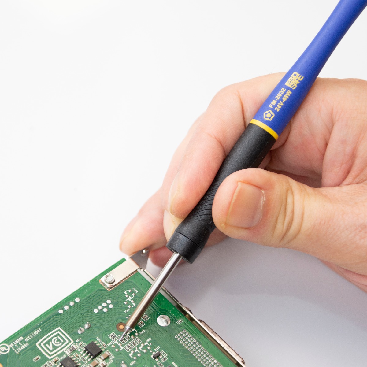
Hakko’s FM-2032 micro soldering iron is a high precision soldering device, which requires experience and skill from the operator. It has been designed exclusively for tiny SMD chip components and features a lightweight, easy grip handpiece to enable the operator to work with greater dexterity under microscopes and magnifiers. The FM-2032 micro-soldering iron is compatible with Hakko’s T30 series of tips, which enable the operator to achieve optimal heat transfer whilst reaching some of the smallest areas on the board. The FM-2032 is compatible with a number of Hakko soldering stations, including the FX-951, FM-203 and FM-206.
- What should I avoid when soldering electrical components?
It is important to avoid ESD (electrostatic discharge), which is the transfer of electric charge that takes place when two objects, which have been charged to different potentials, are brought into contact with one another, brought close together or the di-electric between them breaks down. This ESD can damage the componentry on a PCB and cause product defects as well as equipment failures. The most common example of damage caused by electrostatic discharge is when a charged worker or tool touches a grounded device, which has a low resistance to static electricity. When the tip of a soldering iron comes into direct electrical contact with the pins of a sensitive component, there is a danger of voltage and/or current signal transfer between the grounded iron tip and the grounded PCB, the ungrounded iron tip and the grounded PCB and the grounded iron tip and the ungrounded PCB.
Once electrostatic potential between the two materials is balanced, the ESD event will stop. When soldering components, it is widely assumed that it’s the tip that causes ESD, naturally this assumption is based on the fact that the tip comes into contact with the potentially sensitive device. However, the soldering iron and its tip are just some of the components used at a workbench and other tools like tweezers, wiring, test equipment, etc. can also be sources of ESD as they come into contact with the component or board. ESD events can be detected, measured, and monitored during the soldering process using a variety of diagnostic tools. Hakko produce a range of ESD safe products, which include soldering/rework equipment, wrist straps, protective mats, footwear testers and system testers.
Contamination on parts to be soldered should also be avoided. Any oils, greases and debris make the cleaning of the surfaces to be soldered, by the flux, even more difficult. There are many stages where cleaning may be required, prior to screen printing and soldering in order to remove contaminants from the many previous production stages and after soldering to remove corrosive flux residues. In industry today, many manufacturers are turning to ‘no clean’ processes, implying that cleaning is not required after soldering.
In the ‘no clean’ process, the solids content of the flux is lower than traditional types, however they still contain rosin and activators which are not removed prior to the next process, such as coating or encapsulation of the PCB. Such residues, along with any other unwanted elements collected due to the missing cleaning stage, could cause issues with adhesion and possibly affect the performance of the protecting media applied. For instance, surface contamination due to finger greases and salts, are especially important if the PCB is going to be conformally coated, as any contamination would effectively be sealed within the coating for the life of the product and could cause field failures at a later date. It can therefore be stated that even with advances in modern technologies, such as ‘no clean’ fluxes, cleaning is still an essential part of the multi-stage processes within the electronics industry.
- Is there more than one wire soldering technique?
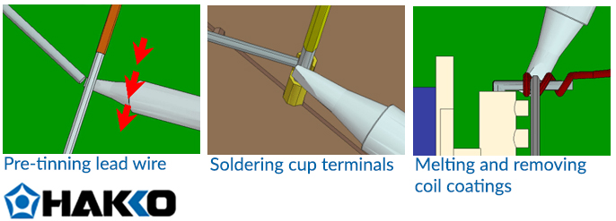
Effectively there is only one wire soldering technique but standard soldering has a derivative, i.e. Drag soldering. This is a technique utilised for longer lines of component leads, e.g. Connectors. Instead of point to point soldering, the tip would not be removed from the connector leads and would be “dragged” down the line of pins whilst simultaneously feeding in additional solder wire. Hakko offers a range of special tips for this technique. These effectively have a concave surface to act as a mini solder wave. As always the process should begin by tinning your soldering tip, cleaning it and then filling the indent with solder.

Apply flux to the leads and pads before soldering. This will help to prevent problems such as solder bridging and insufficient solder. Effectively, the small pocket of solder will be dragged over the pins, heating them and depositing the right amount of solder on each one. Our top tip is to ensure that there is just enough solder in the indent to produce good solder joints. The actual drag time should enable just enough time for a wetting action to occur by gentling gliding the solder over the pins. The trick is to let the solder do the work without any pressure from the soldering iron. A recommended guide for the Hakko Tips available is as follows:- Shape BCM/CM has a hollow section to its cut face, providing high solder retention capability, which is perfect for drag soldering and correcting bridging. Simply feed solder onto the hollow section and drag the tip along slowly.
- Shape BC/C has a shape like a cone or column cut at a slant, which allows users to select the cut surface size depending on the workpiece. It is ideal for drag soldering and pre-tinning of lead wires.
- Shape B is an all-round tip type, which can be used from any direction and is easy to hold at any position. It offers other recommended usages.
- Shape D is very versatile and can be used for multiple works. It has a shape like a flat-blade screwdriver and is capable of soldering by applying the tip in 2 ways: line and face.
- Shape J differs from Shape B by bending the tip end and is capable of soldering by applying the tip in 2 ways: face and point. Lay down the end pad section and drag the tip slowly
- Shape K has a shape like a knife and is capable of soldering by applying the tip in 3 ways: line, face and point. It is used for soldering at narrow pitches, correction of bridging and drag soldering.
- Shape H differs from Shape J by cutting the tip end. It also offers other recommended usages.
There are a number of factors to take into consideration when selecting the most appropriate tip for your application and equipment. For instance, the type of soldering to be done, the HAKKO soldering station and tip series that you are using, as well as the tip shape and size, are all questions to base your selection on. Selecting the most accurate size of tip will significantly improve soldering performance and reduce costs. There are numerous benefits to getting the right-sized tip. Firstly, heat will be more efficiently transferred to the workpiece, which offers easy wetting by the solder. When wetting by solder is easy, the setting temperature can be set to the lowest possible temperature, which in turn prevents tip oxidation and potential damage to your product. This will consequently prolong the service life of the tip and keep manufacturing costs down in the long-term.
We welcome feedback from our customers and potential new customers, so please do talk to one of our team if you have any questions. Look out for next month’s Hakko Tech Tips where we will be providing more advice on how to get the best performance from your Hakko equipment.