No products in the basket.
Dereks Tech Tips – Issue 12

Top Tips to Avoid Common Soldering Pitfalls and Problems
Soldering quality has a huge impact on the performance and functionality of the PCB. In this edition of Hakko Tech Tips, we will highlight some of the most common pitfalls that can happen during soldering to help you avoid specific problems and fully optimise your soldering process.
1) What are the consequences of not keeping the soldering joints sufficiently clean?
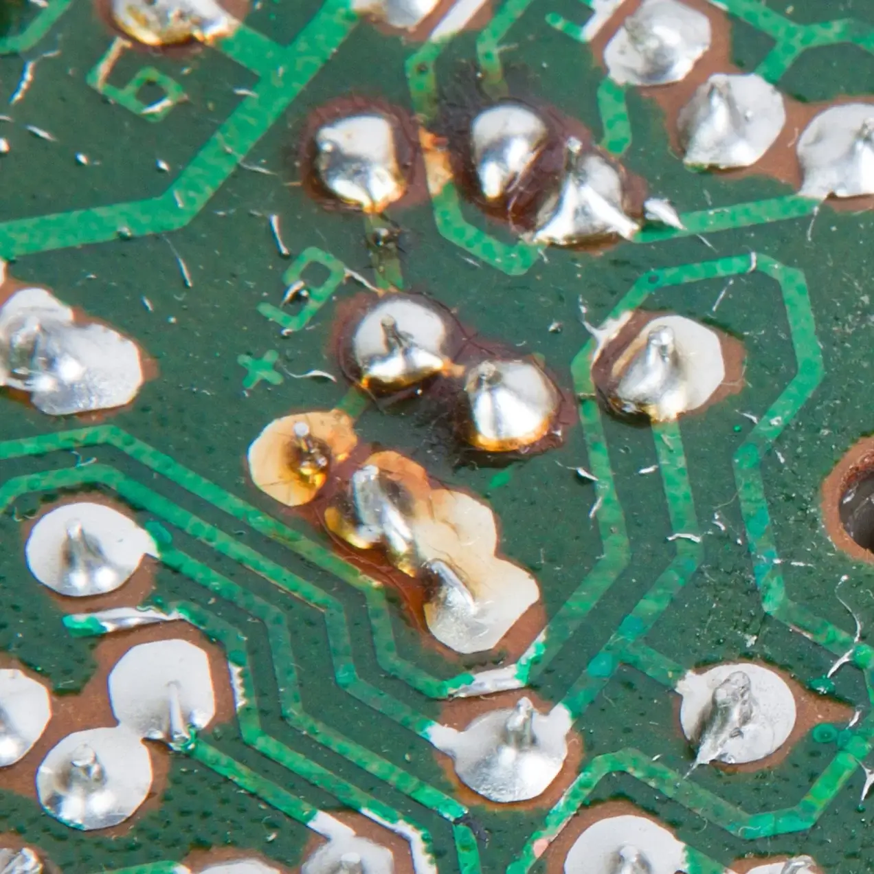
All solder wires initially have an integral flux content, typically 2-3%. Post-soldering, some of this content will have been burnt away. However, upon completion, the soldered joints will have a light coating of flux residue. How visible these residues are will depend on the type of flux used, e.g. Rosin based residues will have a light amber colour so will be easier to identify than a more modern, no clean flux (clear residues). Most modern fluxes can be left on the PCB indefinitely without any short/long term detriment to the product. However, there are instances when the flux residues need to be cleaned off the PCB, e.g. When the assembly needs to be conformally coated or encapsulated. Failure to clean the flux residues from the PCB may then result in the coating/encapsulation materials struggling to adhere to the surface of the soldered joints. Also, if Automatic Test equipment is to be used during manufacture, heavy flux residues can clog test pins leading to “false fail” errors.
2) Is it possible for the soldered joints to fall off as a result of vibration etc. and how can this be avoided – i.e. how do I know that my solder joint is strong enough?
A good quality soldered joint should never “fall off” a printed circuit board as, during the soldering process, an intermetallic layer is formed between the metallisation of the component and PCB. However, some solder alloys have a coarser grain structure which will encourage cracks to form in challenging applications and potentially lead to a catastrophic failure of the solder joint. In such cases there may be a requirement for additional mechanical support for the solder joints, e.g. Encapsulation of the assembly or the application of an adhesive to the base of vulnerable components. If you have any concerns regarding the integrity of soldered joints it may be necessary to seek expert advice and have a selection of soldered joints analysed cross-sectionally. This will indicate if the intermetallic layer is too thick, too thin or just right!
3) Does the quality of the solder joint directly reflect upon electrical conductivity?
Yes, a poor quality solder joint can lead to little or no electrical contact between component and PCB. Solder joint reliability is a very common pain point in electronics design and there are a wide range of factors that impact on the reliability of a solder joint, which can considerably reduce the life expectancy of a solder joint. In some cases this can manifest itself intermittently, potentially leading to a lengthy fault finding process or an embarrassing field failure. It is important to identify the potential causes of joint failure during the design and manufacturing process to help prevent expensive, time-consuming detective work further down the line in a product’s lifecycle.
4) What is a solder bridge and why should it be avoided? What can happen as a result of a solder bridge forming?
A solder bridge is solder content that unintentionally shorts two or more adjacent leads and/or PCB pads. The presence of a solder bridge will usually compromise the intended electrical circuit leading to failure during manufacture. There are numerous measures that can be taken to avoid bridging such as reducing the amount of solder applied in a hand soldering process, altering the stencil design and adjusting print pressure in a reflow process and adding solder mask between the pads when designing the PCB.
5) What are the possible consequences of using too much solder?
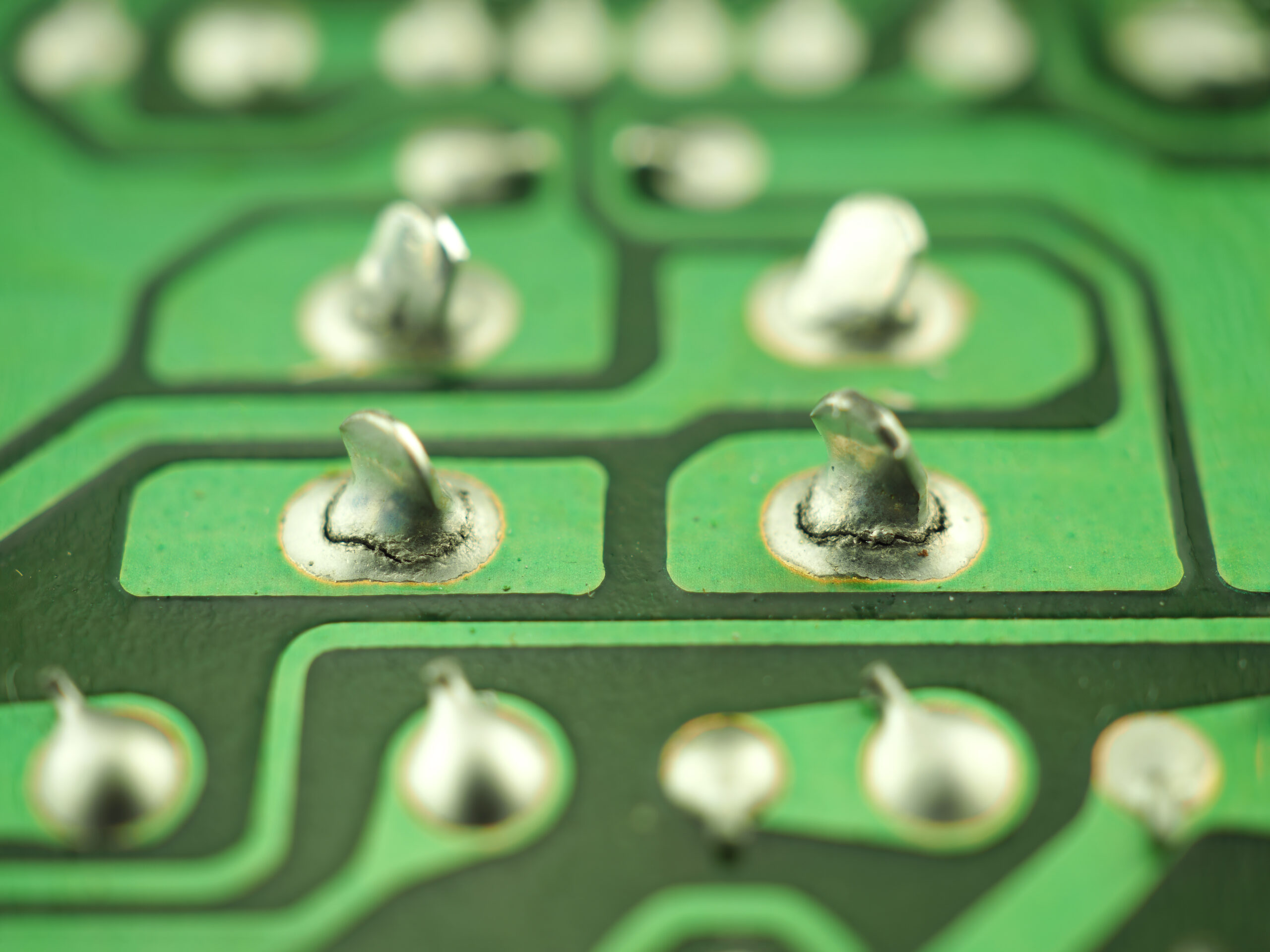
Usually caused by delayed removal of the solder wire during the hand soldering process, the use of too much solder can cause many issues, e.g. Solder bridges. However, these are fairly easy to identify for the trained eye. The main problem with excessive solder is that it masks the component lead and PCB pad, thus preventing a close inspection of the joint in question. This can hide a multitude of potential issues, e.g. Insufficient wetting. The optimum amount of solder alloy should always display a generous flow covering the complete outline of the PCB pad and the upper portion of the component lead with a concave fillet/meniscus of solder.
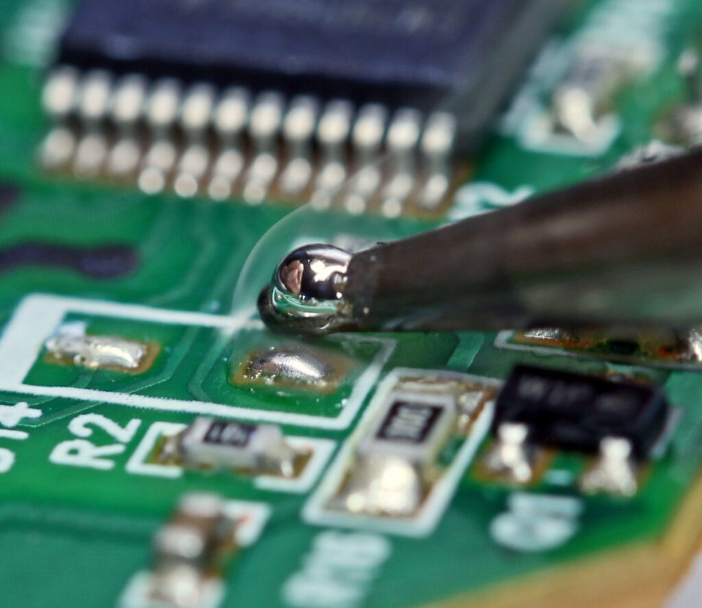
6) What are solder balls and how are they formed – i.e. what are the most common causes?
As the name would suggest solder balls are tiny spheres of solder alloy. Amongst other reasons, these can be caused by rapidly heating any moisture or flux content present. If not stored correctly, over time, moisture can be absorbed into a PCB. Another source of moisture could be the flux present in any soldering process. In hand soldering, the application of a soldering iron at 380 °C (typically) can inevitably cause the water/flux content to boil thus producing a violent reaction which will disperse the molten solder in and around the intended solder joints. Because of the surface tension of the molten alloy these smaller amounts of solder will manifest themselves as solder balls.
7) Cold solder joints occur as a result of insufficient heat being transferred. What is their appearance and what can occur as a result of this?
Cold solder joints can be identified by insufficient wetting and can lead to poor conductivity/reliability. The root cause is insufficient heat being applied during the soldering process. However, this in turn can be caused by many different issues, e.g. Inefficient soldering equipment, incorrect temperature set point of the soldering equipment, insufficient application of heat by the soldering iron (with respect to the time delay) and finally PCB design. Many of today’s modern PCB designs require multiple layers with heavy, integral ground planes. These have a massive heatsink effect and can absorb significant amounts of heat.
8) How do overheated solder joints appear and how can these be avoided? Is it possible to completely ‘kill’ the PCB as a result of overheating a solder joint
When too much heat is applied to a solder joint this may or may not be immediately apparent. Initially the flux residues are likely to caramelize and harden giving a poor visual appearance. The next scenario would be to produce a joint with an intermetallic layer which is too thick. Whilst not apparent to the naked eye this would produce a brittle joint which is likely to result in a field failure. Ultimately, if a really excessive amount of heat is applied this would damage or destroy both the component and PCB, e.g. Lifting of PCB pads/tracks.
9) What is a tombstoned component and how do these appear? Is it possible to avoid this phenomenon?
Tombstoned components are when one end of a device is soldered to the PCB and the other is not in contact. It is a phenomenon more associated with a reflow soldering process and is caused by the surface tension of the molten solder lifting one end of the device. If there is any imbalance in component alignment the forces exerted on each end of the device would be unequal and result in lifting the end with the least force.
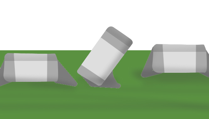
Tombstoning is a major concern, quite simply because it creates a disconnection on the PCB. There are a number of factors that can cause Tombstoning, including unevenly applied solder paste, thermal inequalities between solder joints, inadequate pad designs – either too big or too small, and ground plane circuit board designs.
10) Joints that are not fully wetted form a poor connection with the board. How is this best avoided?
The soldering process is a skilled practice and if there is any doubt about the integrity of the soldered joint then closer inspection is required. Visually you can establish if there has been sufficient wetting of the surfaces to be joined, i.e. The component and PCB. However, this only gives a surface analysis. So a more in-depth analysis for proving joint integrity is by cross-sectional analysis which, when examined under a microscope, will confirm the metallisation/interfaces of the joint thus establishing if the joint is good or not. Causes of poor/insufficient wetting can include oxidation of the component/PCB, poor selection of solder wire/flux materials, insufficient heat applied to the soldered joint, i.e. With respect to temperature and time.
We welcome feedback from our customers and potential new customers, so please do talk to one of our team if you have any questions. Look out for next month’s Hakko Tech Tips where we will be providing more advice on how to get the best performance from your Hakko equipment.